As Moore’s Law slows, the semiconductor industry is increasingly turning to advanced packaging to maintain the trajectory of performance gains. The transition from monolithic scaling to chiplet-based architectures has made heterogeneous integration and high-density interconnects essential. At the heart of this evolution lies an equally critical question: How can we package these complex systems efficiently, reliably, and cost-effectively?
One of the most promising answers comes from micro 3D printing, a revolutionary additive manufacturing approach that is transforming how semiconductor packaging substrates, interposers, and RF components are designed and fabricated. Unlike traditional subtractive manufacturing methods, micro 3D printing offers unprecedented flexibility, speed, and miniaturization capabilities—paving the way for a new era of high-performance, cost-effective packaging.
The Promise of Micro 3D Printing in Semiconductor Packaging
Micro 3D printing leverages high-resolution techniques such as Projection Micro Stereolithography (PμSL) to build complex three-dimensional microstructures layer by layer. With resolutions down to 2 μm and materials spanning polymers, ceramics, this technology enables the fabrication of fine features, non-planar geometries, and integrated passive/active structures that were previously difficult or impossible to achieve using traditional lithography.
In semiconductor packaging, this capability is particularly valuable for:
1.Creating fanout interposers with customized through-holes and redistribution layers
2.Integrating antenna-in-package (AiP) systems with optimized signal paths
3.Rapid prototyping of advanced package substrates with embedded RF components
4.Reducing the number of process steps and avoiding photomask costs
Let’s explore how recent research demonstrates the power of this technology to reshape packaging.
Case Study 1: Curved Through-Hole Interposers for Advanced Packaging
DOI 10.1109/ECTC51687.2025.00201
In the paper titled “3D Printed Fanout Interposer Substrates with Curved Through-Holes for Rapid Prototyping of Advanced Packaging”, researchers developed a novel organic interposer using micro-3D printing with embedded curved through-hole vias. This design aims to tackle the limitations of conventional redistribution layer (RDL) manufacturing, which requires over ten lithographic steps per layer and often becomes cost-prohibitive for small-scale or prototype production.
This advancement is expected to provide new opportunities for small-entity chip packaging, facilitating rapid validation and integration of heterogeneous devices in advanced electronic systems.
Key Innovations
Curved Through-Holes: Departure from conventional redistribution layer (RDL)-based build-up layers, the curved introduces the potential to connect chips with I/O interfaces of varying pitches, enhancing design flexibility, allowing for high interconnect density and signal integrity
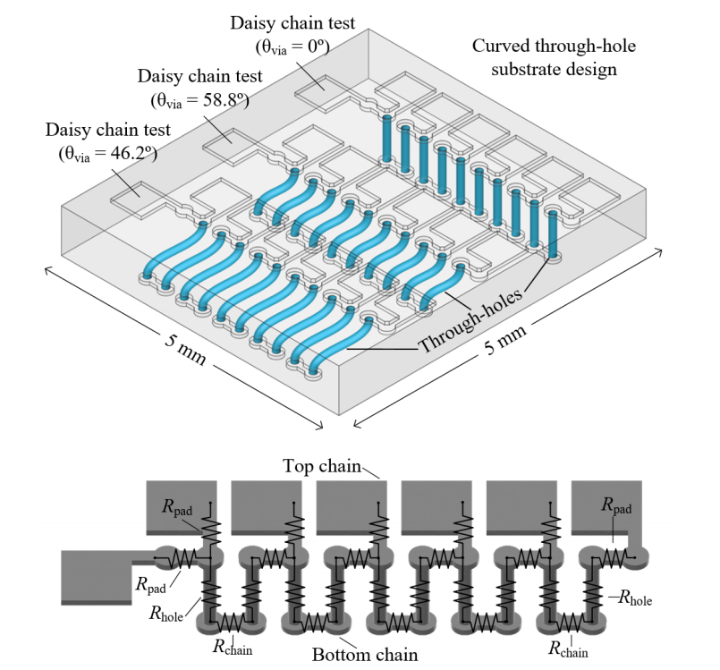
Fig. 3D CAD design of daisy chain pattern along the continuous through-holes with contact pads.
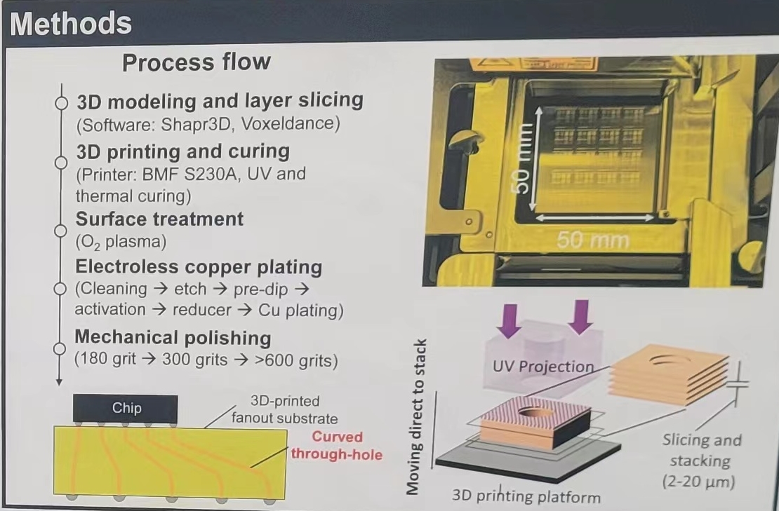
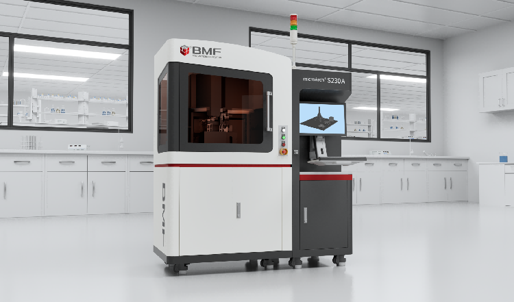
High-Fidelity Fabrication: Using BMF microArch® S230A(resolution:2μm)3D system, structures were printed with high accuracy
One-Step Metallization: A recessed pattern and electroless Cu plating process enabled the formation of conductive paths with <1 Ω resistance and <0.5 dB insertion loss up to 40 GHz.
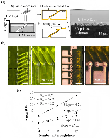
Fig. 3D CAD design of the substrate
Impact on Packaging
This approach simplifies interposer production by consolidating multiple fabrication steps into a streamlined additive process. More importantly, it enables rapid prototyping of new interposer layouts, low-cost scaling for specialized applications.And enhanced RF performance due to low-loss, high-integrity metallization.
The compatibility with Cu pillar bump bonding ensures seamless integration into existing semiconductor assembly lines.
Case Study 2: Quasi-Coaxial Lid Substrates for AiP
DOI 10.1109/ECTC51687.2025.00302
In the recent study, “Quasi-Coaxial Through-Hole Integrated Additively Manufactured Antenna-in-Package Lid Substrates”, the authors introduced a lid-type AiP substrate integrating a patch antenna, coplanar waveguide (CPW), and quasi-coaxial vias, all fabricated through additive manufacturing.The proposed 3D-printed lid substrate with embedded RF components offers a cost-effective and scalable solution for AiP substrates.
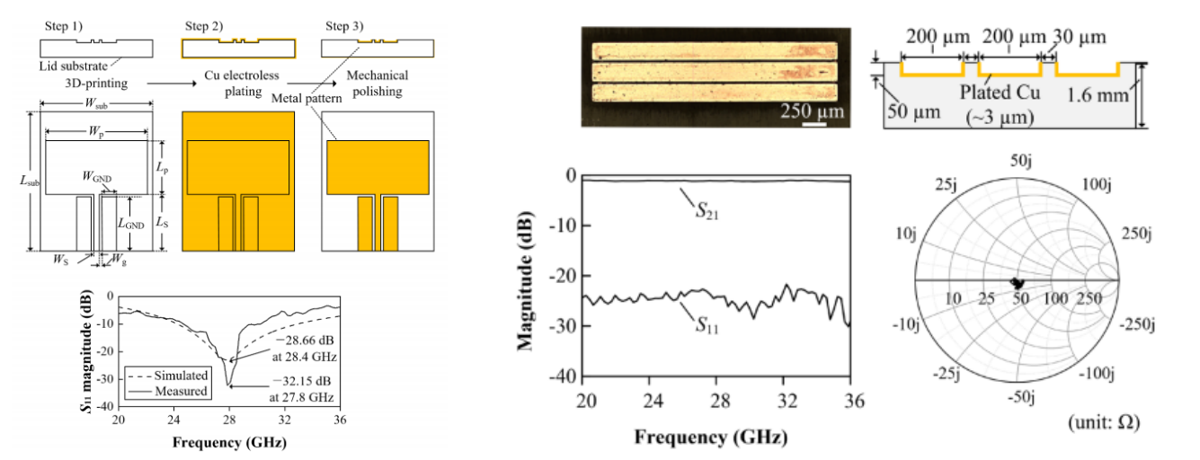
Fig. Schematics of the fabrication flow and top views of a patch antenna on a 3D-printed substrate.An optical microscope image of a CPW line on a 3D-printed substrate and the cross-sectional schematic.
Design Highlights
Quasi-Coaxial Through-Holes: The signal via is surrounded by multiple GND vias, creating a coaxial-like waveguide that suppresses EMI and ensures 50-ohm impedance matching.
Full RF Integration: The patch antenna, CPW line, and chip cavity were co-fabricated, enabling compact and high-performance AiP. Using BMF microArch® S230A(resolution:2μm)3D system, researchers produced a 5×7 mm polymer structure with a 1.6 mm thickness and 200 µm via diameter.
Precise Electromagnetic Tuning: The designed lid substrate exhibited resonance at 27.94 GHz with GND metal plane to mitigate the EMI to underlying dies.
Micro 3D printing complements, rather than replaces, existing semiconductor processes—especially for applications where customization, space optimization, and electrical performance are paramount.
Conclusion
As the industry races toward higher performance, lower power, and more compact solutions, packaging is becoming the central battlefield. Micro 3D printing offers a new paradigm—one that combines precision, flexibility, and speed. By enabling unprecedented structural freedom and integrating complex RF and digital pathways in a single substrate, this technology is set to redefine how we approach semiconductor integration.
Companies and research institutes that embrace micro-3D printing today will be the ones shaping the chiplet-driven, AI-powered, RF-enabled world of tomorrow.To learn more about how BMF’s PµSL can help the semiconductor industry, visit our overview page or request a benchmark part.
