Things are getting smaller, whether it’s connectors inside a phone or components inside a medical device, and that trend for miniaturization is happening. Those traditionally used to produce those things are being challenged. A lot of things in our world are getting smaller and the manufacturing methods that are traditionally used to produce those things are being challenged. So, micro 3D printing becomes even more viable as a choice for high-end precision manufacturing fields, including precision electronics production.
The Importance of Micro-Integration in Precision Electronics
With the qualification of new materials and the miniaturization movement, micro 3D printing is in a unique position to achieve high-precision, miniaturized, customized manufacturing, allowing electronic engineers to quickly make prototypes and greatly improve R&D and experimental efficiency. The fact is that engineers can print very small features with high resolution, and high tolerance capability. Also, they can print rather large batches, which allows them not only to do some fundamental and really hardcore R&D, but also to kind of already start scaling up when they get a prototype that works.
- High-precision resolution:Micro 3D printing technology can achieve precision at the micron level, which is crucial for the manufacturing of precision electronic components.
- Complex structure manufacturing:Micro 3D printing technology can create complex internal structures that are difficult to achieve with traditional methods, such as micro-channels and micro-chambers.
- Design freedom:Provide engineers with innovation and design freedom to help design electronic components with better performance and faster iteration.
- Rapid prototyping:Rapidly manufacture prototypes, accelerate the R&D process and shorten the time to market.
- Customized production:Meet the needs of specific applications to enhance the adaptability and competitiveness of products.
- Material diversity:A variety of materials can be used, including resins, ceramics, and a variety of post-processing methods can be adapted, providing more possibilities for the manufacturing of electronic components.
- Reducematerial waste: As an additive manufacturing technology, micro 3D printing reduces material waste and costs.
- Integrated design:It can achieve integrated design of electronic components, integrating multiple functions into a miniaturized device.
BMF Precision Electronics Applications
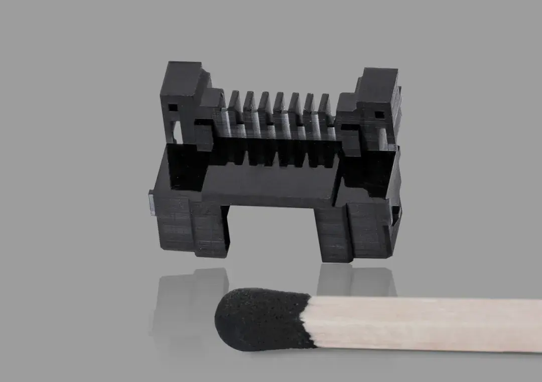
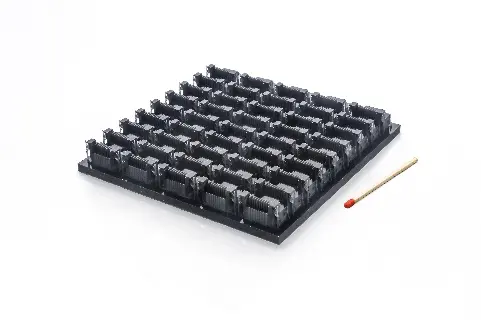
RJ Connector
Printing equipment: microArch® S140 (resolution: 10 μm)
Dimensions: 16.7 * 9.55 * 9.36 mm³
Minimum wall thickness: 0.14 mm
Minimum spacing: 0.28 mm
BMF’s PμSL technology meets the requirements for high efficiency and customization, effectively solving the problem of long processing cycles and high processing costs for precision connectors. In addition, it can be produced in rather large batches.
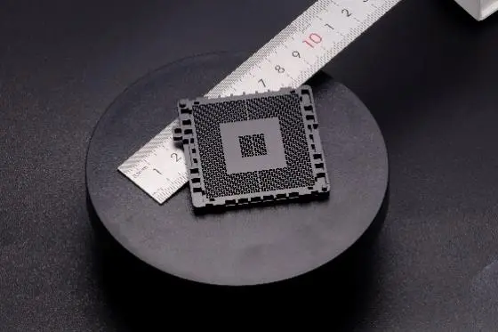
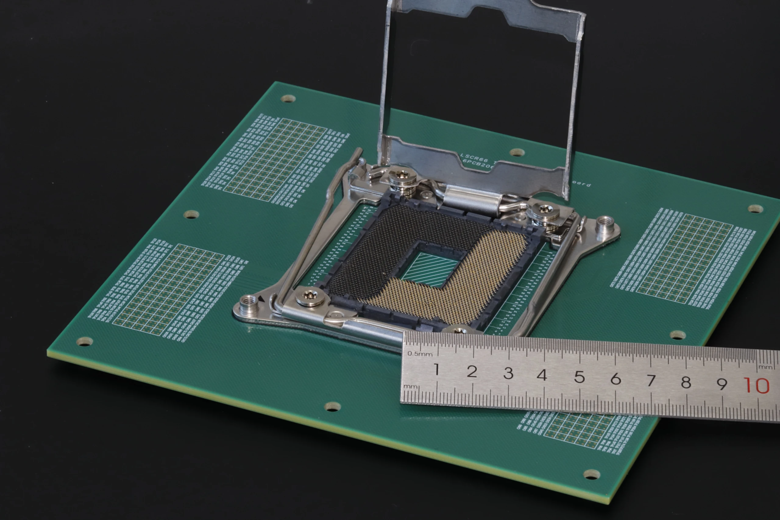
Chip Array Socket
Printing equipment: microArch® S240 (resolution: 10 μm)
Dimensions: 51 * 5.85 * 59.74 mm³
Minimum spacing: 0.23 mm
While ensuring key precision, it significantly shortens the production cycle, reduces the cost of prototype testing, and greatly improves the response speed during the product development stage, which also provides a high transmission rate and high-quality processing solutions for the semiconductor industry.
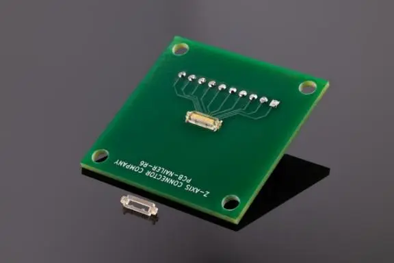
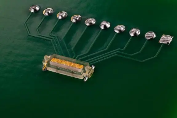
High-Heat Resistant Connector
Printing equipment: microArch® S230 (resolution: 2 μm)
Application: Z-Axis Connector Company is a leading privately held corporation specializing in connector manufacturing. With BMF’s open platform, Z-Axis was able to use 3D Systems Figure 4® HI TEMP 300-AMB material, and engineered a tiny and delicate structure to withstand temperatures up to 300°C.
BMF’s PμSL and Hybrid Resolution 3D Printing Technology can effectively simplify the verification process from design to manufacturing for engineers, significantly shorten the R&D cycle, and reduce production costs. It will promote the innovation of artificial intelligence, 5G, semiconductor and other industries, and meet the demands of modern electronics.
If you are interested in discussing electronic applications with a member of the BMF team, please contact us. (https://bmf3dapac.com/#contact)

